
Before Computer Aided Design, there was CAD, Cardboard Aided Design. I present to you: Computer Aided Cardboard Aided Design, where we use CAD to design it, CAD to test fit it, and finally CAD again to make adjustments based on the issues found with the CAD. I hope that clears things up for you.
This is a quick guide on how to export files from KiCad that can be used on a 3D printer or laser cutter, so you can get truly accurate mockups for test fitting before you pull the trigger on the real thing.
Getting a printable outline from KiCad is super simple - just open up the PCB editor and hit the print icon in the toolbar! But if you're looking to get a mockup of the PCB that's sub-millimeter precise, manually shaping a piece of paper with a pair of scissors just isn't going to cut it.
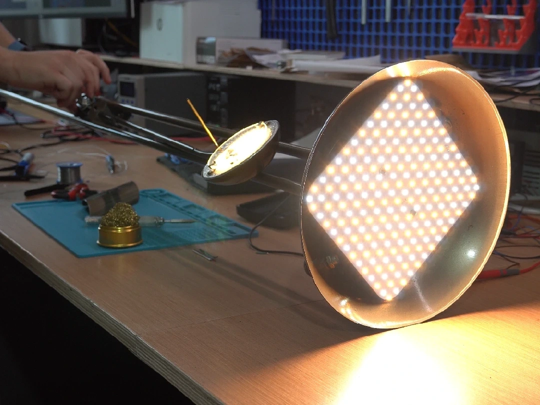
For the lamp PCB it was important for me to ensure that the screw holes were precisely lined up, and that the PCB didn't touch the edges of the "bowl" - the outer shell of the lamp.
Firstly, rigidity - a piece of paper flops around, so I wanted something that kept its form, as it's a complex shape to fit.
Second, while I'm sure I could have done a pretty good job with a pair of scissors, using a machine to cut the holes to their precise diameter and location made sure that everything screwed together properly. It's easy to rip and deform the paper when you need to make a hole in the middle of it.
3D printing the board
KiCad is able to export a 3D model file straight from the menu. Head to File > Export > STEP/GLB/[...].
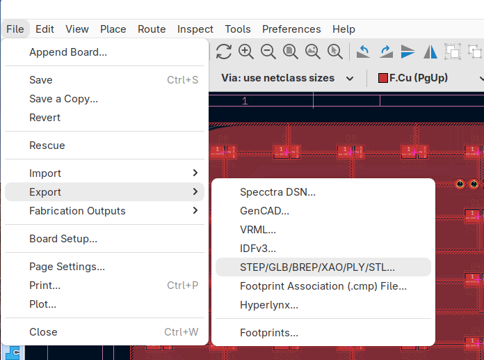
While it's possible to get a 3D model that includes all the components within it, you'll end up with a very large filesize, something that takes a lot longer to print, and the printer will struggle getting the detail of the smallest components. It might be helpful if you've got a few large components that you need to ensure fit in your design, but for this guide, we're only interested in the board itself.
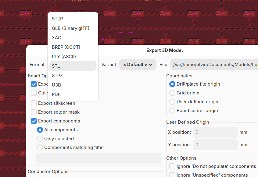
First off, switch the format to STL. This will produce a mesh object that is best suited to 3D printer slicers.
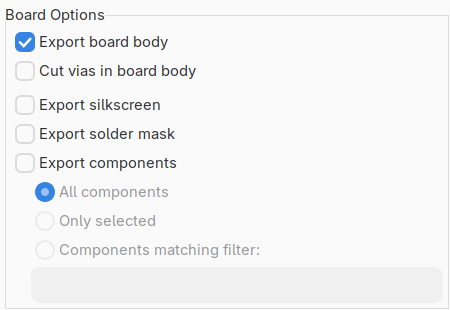
Next up, make sure to only select "Export board body". The default will also export the components, which is what I talked about at the start of this section.
Set the File: section in the top right as the place to export it to, and you'll have a 3D model file you can open up directly in your slicer of choice. Here's what it looks like in Prusa Slicer:
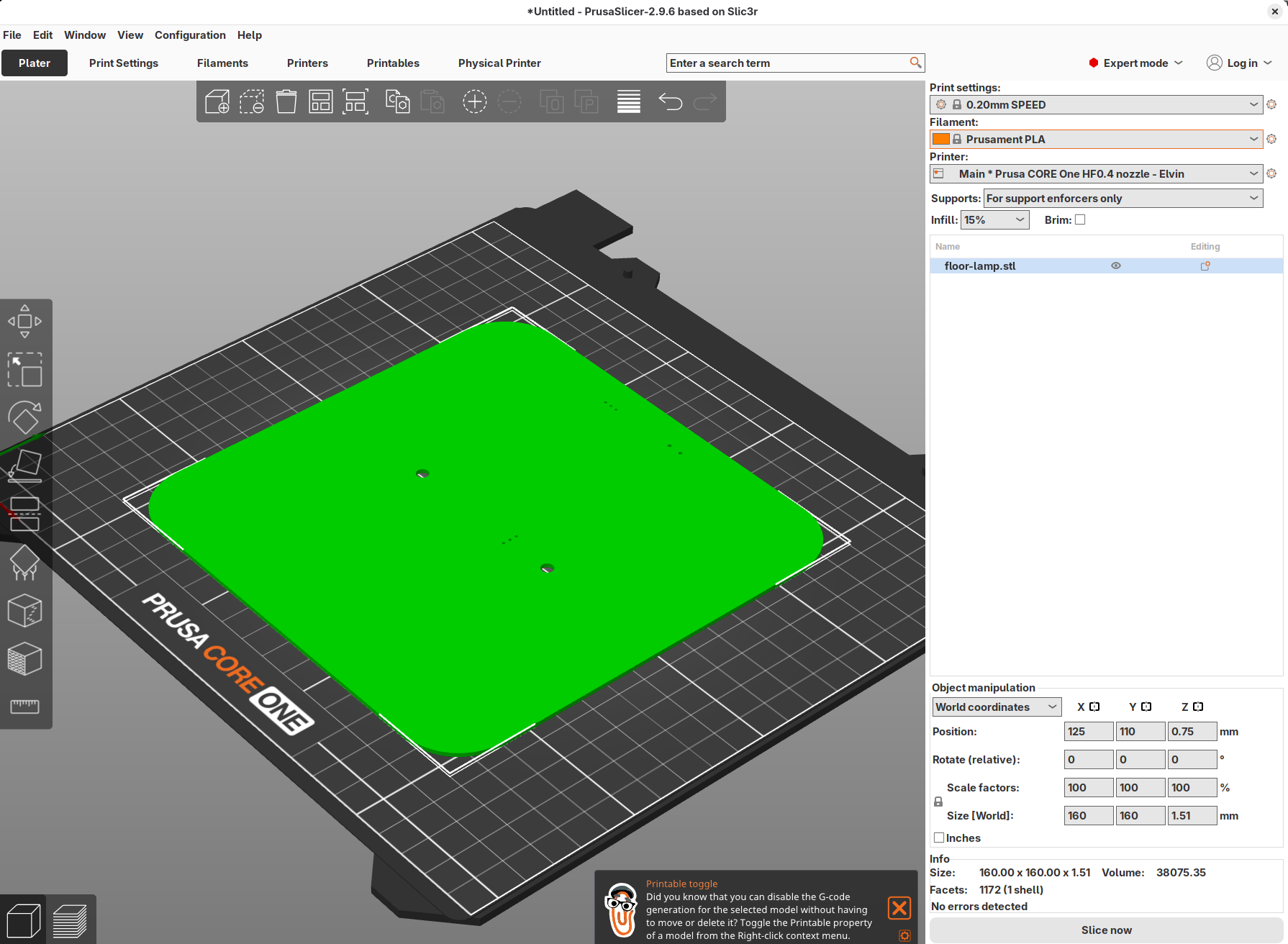
Make sure you set the layer height to 0.2mm to ensure that the height of the PCB comes out correctly. The model also includes the holes for screws and through-hole components.
One thing to note is that FDM 3D printers are not good at perfectly sharp outer corners, and inner corners might not match what the PCB fab can do with its drill bits. I would recommend ensuring that all corners have at least a 1mm corner radius in KiCad, so you don't risk having the PCB catching the corners of your design when the real one arrives.
This is the method I used when first mocking up the design of the PCB for the CTRL ONE. The PCB needs to slide into the housing at an angle, where it's then locked into place by rails on the edge of the enclosure. This kind of fitment is something you need to feel, not just see, so 3D printing the outline of the board allowed me to align the fit and feel before I even started designing the layout of the components on the board.
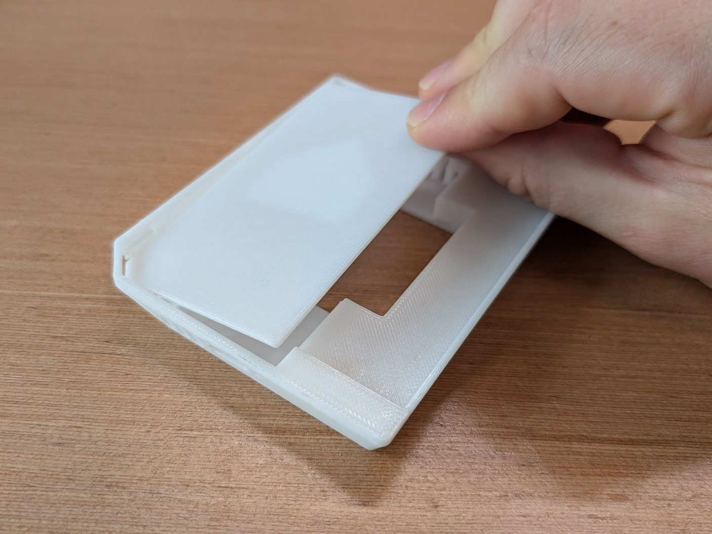
The CTRL ONE is a smart room controller and thermostat with a touchscreen, ePaper display. Designing and creating it is how I learned everything in this guide. The add-on interface is completely open for you to build your own add-ons to make it fit your home, and these techniques can help you make sure it fits in the back of the CTRL ONE before you spend the big bucks at the PCB fab.
Laser cutting the board
For a laser engraver, we need to have a 2D file instead of a 3D one. The benefit of this method is that a laser is a lot faster and far more precise with much crisper edges and corners. You can also engrave the footprints, just like with a normal printed piece of paper. On the flipside it's much less likely that you have a laser cutter, and you'll need to have a material on hand that matches the thickness of the final PCB. For my use-case the thickness didn't matter (only the rigidity) so I just found a 1mm piece of cardboard.
While the print option gives us something that works on a piece of paper, laser engraver software such as LightBurn expects a vector file such as an SVG. This turns the PCB into a series of lines that we can feed into the software used by the machine.
KiCad is completely capable of doing this as it's the basis of what's used in the PCB manufacturing process itself.
First, head over to File > Fabrication Outputs > Gerbers.
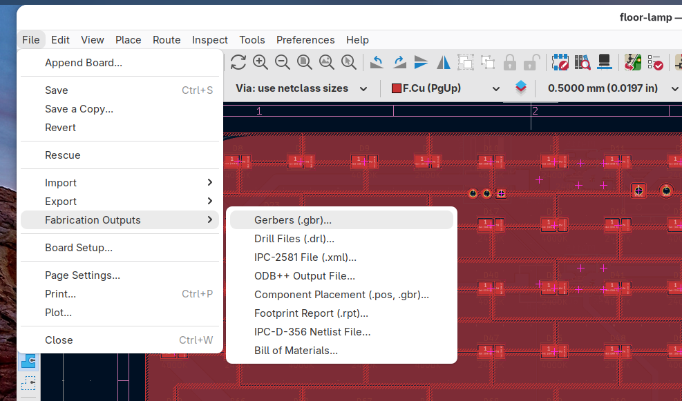
For mockup purposes we only need some basic parts. We can also etch in the location of components, so you can visually see where they sit.
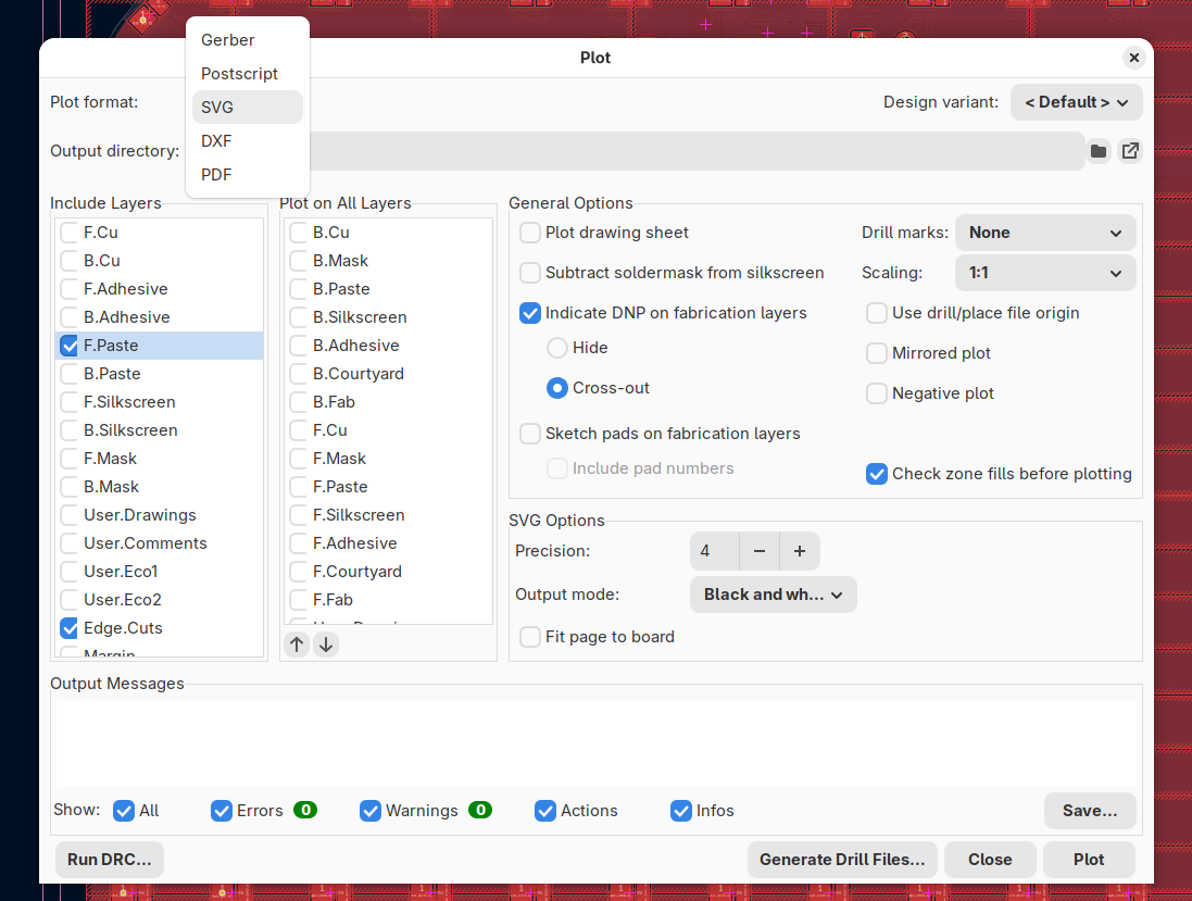
First, in the plot format menu, change the plot format to SVG. This gives us a universal vector file format that works in other software.
Next up, in the "Include layers" section, select Edge.Cuts. This will give you the outline of the board. If you're also looking to engrave details, then using F.Paste will give you the pads that the components will be soldered to.
You might also find F.Silkscreen useful if you've got writing or markings that you want to display, but do note that letters and numbers come out as a single line, which means that it'll come out much thinner on a laser engraver than it would be on the actual PCB.
Choose an output directory and hit Plot. You'll get a series of SVGs, one for each selected layer.
Open up LightBurn and drag in all the SVGs at once. This will ensure that they're perfectly stacked on top of each other, like so:
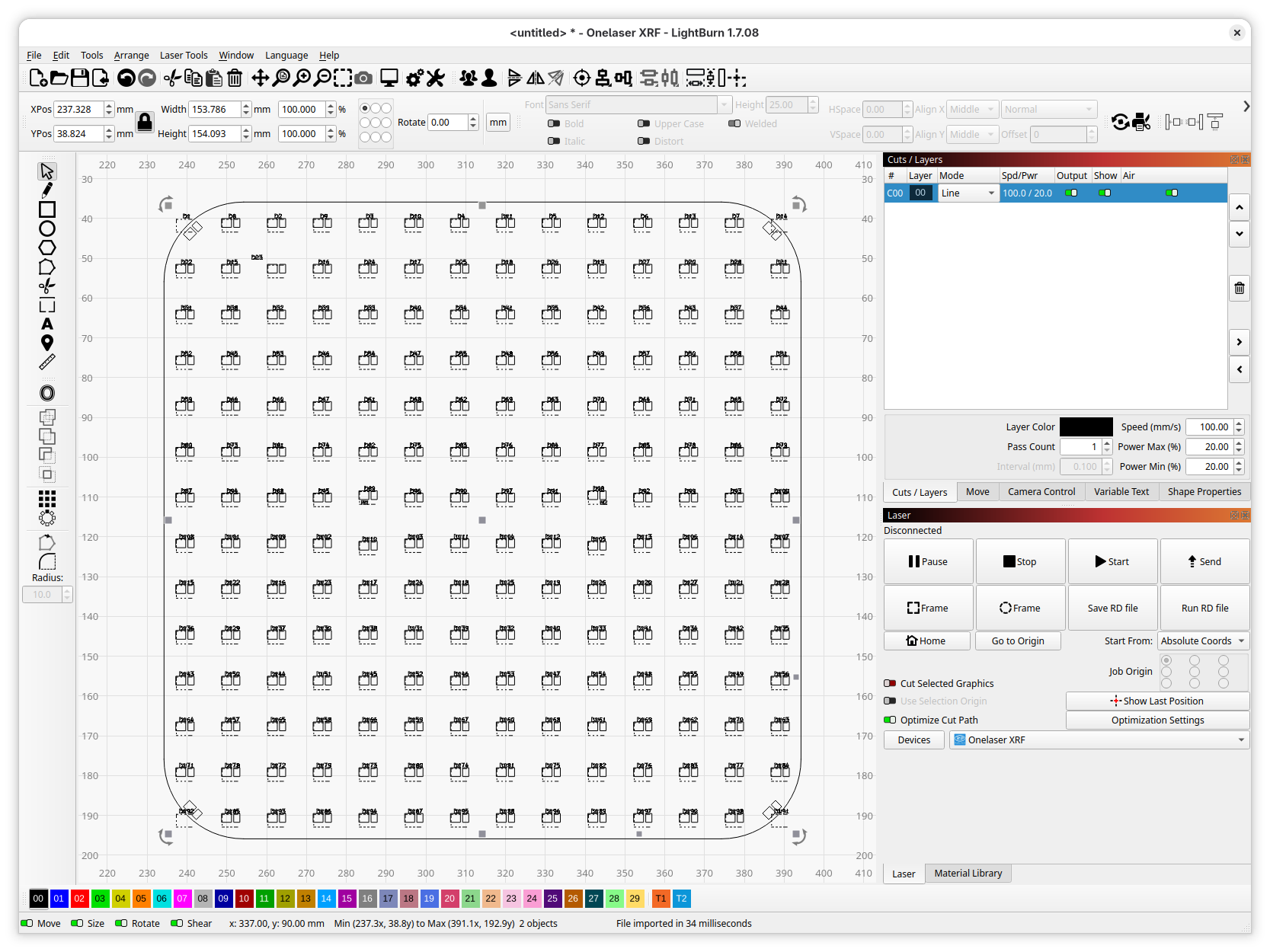
From here it's time to dial it in according to your material. Edge cuts and footprints come out fine, but silkscreen will need a little cleanup:
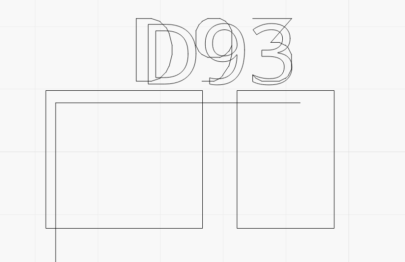
This can all be handled within LightBurn. Go through and delete the lines you don't need.
You'll also see that the screw holes are missing. As they don't count as edge cuts, they're not in the final output. A quick hack is to go back into KiCad, and select the Edge.Cuts layer. Add a circle that perfectly matches the mechanical hole.
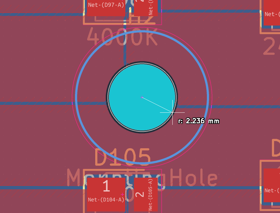
Export the layer again, and make sure to clean up the added circles once you're done.
From here, I leave it to you! Dial in each layer according to the material and how you want the machine to cut/engrave, and get a perfectly shaped mockup PCB for your next project.